TSMC is embedding Nvidia's AI and accelerated computing across its most complex fab operations, from lithography to defect inspection, in a collaboration that could reshape semiconductor manufacturing economics.
Back
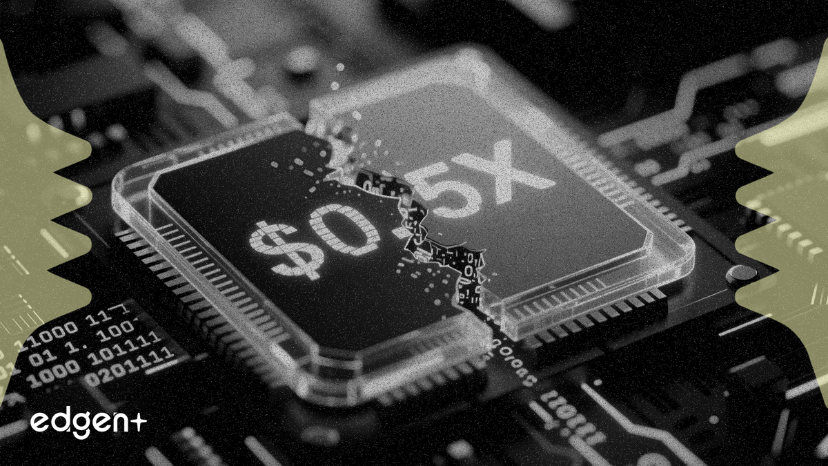
Nvidia and TSMC bring AI into fabs, cutting lithography costs 50%
TSMC is embedding Nvidia's AI and accelerated computing across its most complex fab operations, from lithography to defect inspection, in a collaboration that could reshape semiconductor manufacturing economics.
Nvidia's CUDA-X libraries and AI models are now powering TSMC's lithography, process simulation and defect inspection workflows, delivering a 20% to 50% improvement in lithography cost effectiveness and 50x faster chemistry simulations for semiconductor material design.
"TSMC is bringing NVIDIA AI and accelerated computing into the fab itself, tackling some of the world's most complex design and manufacturing challenges," Jensen Huang, founder and chief executive officer of Nvidia, said.
The collaboration spans four areas of fab operations. TSMC is using Nvidia's cuLitho library for computational lithography — the printing method for chip mask design — achieving a 20% to 50% improvement in cost effectiveness or cycle time versus CPU-based approaches. The cuEST library accelerates electronic structure simulations for semiconductor material design by an average of 50x. For process control, Nvidia's cuML machine learning library helps TSMC distill hundreds of thousands of process parameters across thousands of steps into precision inputs for ML models, reducing process variation. On the fab floor, Nvidia H200 GPUs are powering scheduling computations that improve fab productivity.
The deeper integration of AI into semiconductor manufacturing validates a thesis that has driven the Philadelphia Semiconductor Index up 89% year to date: AI infrastructure spending is broadening beyond GPU design into the tools, materials and processes that underpin chip production. TSMC expects its AI chip business to grow at roughly 60% compounded annually from 2024 to 2029, while Nvidia has projected data center capital expenditures will reach $1 trillion by 2027.
Defect Detection and the Virtual Fab
Beyond core manufacturing, TSMC is deploying Nvidia's Metropolis platform and TAO Toolkit for automated defect inspection using vision AI, improving detection of nanometer-scale defects while reducing the need for repeated labeling and retraining as process conditions change. The company is also exploring Nvidia's Omniverse libraries to build FabTwin, a virtual fab environment for evaluating process tool layouts and simulation workflows before physical implementation — a shift that could reduce the capital commitments required for new fab construction.
The Cost of Going Global
The collaboration comes as TSMC navigates a costly geographic expansion. The company pushed its full-year 2026 capital expenditures to the high end of its $52 billion to $56 billion range, with overseas fab construction in Arizona, Japan and Germany costing an estimated 4x to 5x more than identical facilities in Taiwan. TSMC management has said overseas fab expansions and the ramp of next-generation nodes will trigger a 2% to 3% gross margin dilution starting in the second half of 2026 and extending into 2027. The efficiency gains from AI-optimized manufacturing could help offset some of that pressure, though the scale of the margin headwind is material relative to TSMC's current gross margins.
For investors, the collaboration reinforces Nvidia's competitive moat — its CUDA ecosystem is becoming embedded in industrial hardware workflows beyond data centers, extending its addressable market into semiconductor capital equipment. Nvidia shares trade at roughly 35x forward earnings. TSMC, at 26x forward earnings, offers a lower-beta way to play the same trend, though margin dilution from overseas expansion warrants monitoring. The broader beneficiary may be the semiconductor equipment and memory supply chain, where equal-weight ETFs like the Invesco Semiconductors ETF have returned 105% year to date as AI spending broadens beyond megacap chip designers.
This article is for informational purposes only and does not constitute investment advice.
[1] NVIDIA and TSMC Bring AI Into Fabs to Advance Semiconductor Design and Manufacturing[2] Nvidia Says Big Tech Will Spend $1 Trillion in Capital Expenditures in 2027: 3 Stocks to Buy If It's Right[3] Taiwan Semiconductor Manufacturing (TSM): Leopold Aschenbrenner Takes Bearish View[4] The Semiconductor Play Nobody Owns Just Lapped Wall Street’s Biggest Names
© 2026 Edgen Powered by