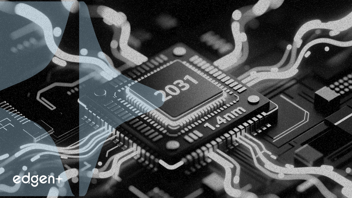
Huawei Technologies Co. has proposed a new semiconductor principle that aims to match the transistor density of a 1.4-nanometer process by 2031, a move that could challenge the industry’s reliance on traditional geometric scaling. The new principle, dubbed “Tao’s Law,” suggests using “logical folding” to achieve performance gains, potentially creating a new path for chip advancement outside the established Moore’s Law trajectory.
“This is the first time China has proposed a new principle to guide the development of the global semiconductor industry,” the People’s Daily reported, highlighting the national significance of the announcement. The law suggests replacing “geometric scaling” with “time scaling,” a concept that appears to focus on architectural innovation rather than simply shrinking the physical size of transistors.
Details of the technology remain sparse, but the strategy aligns with Huawei’s recent successes in engineering around US export controls. The company recently unveiled a 122TB solid-state drive that uses an advanced Die-on-Board (DoB) packaging technique to achieve 33% higher density from less advanced memory chips. This focus on packaging, a key bottleneck for the entire AI industry, shows a clear pattern: when cut off from the most advanced components, Huawei innovates in architecture and integration to remain competitive.
If viable, “Tao’s Law” could have a significant impact on the global semiconductor market. It represents a strategic effort to bypass the need for extreme ultraviolet (EUV) lithography machines, which are restricted from being sold to China. A successful outcome would be bullish for China’s tech sector and create competitive pressure on market leaders like TSMC, Samsung, and Nvidia, whose roadmaps are heavily invested in the capital-intensive geometric scaling model.
A Two-Pronged Strategy
Huawei’s approach demonstrates a two-pronged strategy to achieve semiconductor self-sufficiency. On one front, as seen with its OceanStor Pacific 9926 all-flash arrays, the company is maximizing the potential of existing hardware through advanced packaging. By mounting NAND flash dies directly onto the circuit board, Huawei can build a 122 TB SSD that is competitive with drives from rivals using more advanced memory.
On the other front, “Tao’s Law” represents a more fundamental, long-term bet on a new design paradigm. Instead of fighting a losing battle for access to sanctioned EUV tools, Huawei is attempting to rewrite the rules of the game. This turn to architectural innovation is part of a broader industry trend exploring post-silicon technologies, including the light-based photonic switches being developed by researchers at the University of Pennsylvania and Montana State University to enable faster, more efficient computation.
For investors, Huawei’s announcement is a high-risk, high-reward proposition. The 2031 timeline underscores that this is not an overnight solution, and the technical viability of “logical folding” on a mass scale is unproven. However, it signals a clear and determined strategy from a major technology firm to innovate around geopolitical and physical limitations. Any verifiable progress on this path could force a re-evaluation of the long-term competitive landscape in the semiconductor industry.
This article is for informational purposes only and does not constitute investment advice.